Materials Discovery
Research in the Materials Discovery subgroup of the Mirkin group focuses on the development of novel scanning probe-based lithography techniques and the application of these techniques to address questions in a variety of fields, including surface science, nanoelectronics, biology and medicine, materials synthesis and discovery, and catalysis.
Selected Techniques
Dip-Pen Nanolithography (DPN)
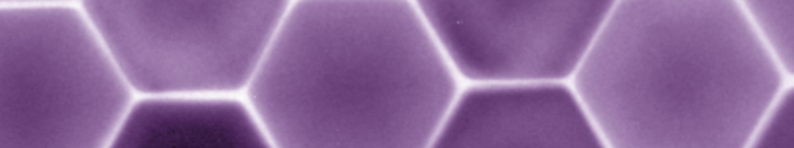
Dip-pen nanolithography (DPN) was invented and introduced in 1999 by the Mirkin group, and it can be used to deposit molecules and materials on surfaces with sub-50 nm resolution. This method employs an atomic force microscope (AFM) probe “pen” coated with a molecule- or materials-based “ink.” Upon contact with a surface, the ink is deposited to the substrate via diffusion through a meniscus that forms between the tip and substrate under ambient conditions (Figure 1). In initial demonstrations, small organic molecules, such as alkanethiols (e.g., octadecanethiol (ODT) and mercaptohexadecanoic acid (MHA)), were written onto gold substrates; these molecules were chosen for their ability to form well-ordered self-assembled monolayers (SAMs). Since then, DPN has been used to write or template many types of molecules and materials (e.g., polymers, colloidal nanoparticles, sol-gel precursors, biomolecules including proteins and oligonucleotides, and single virus particles and bacteria) on a variety of surfaces (including metals, semiconductors, and insulators) by controlling various experimental parameters, including humidity, writing speed, and dwell time. Conventional DPN is a serial process, and it is lower in throughput than stamping or optical lithography-based techniques. However, the throughput of DPN was increased by parallelizing the deposition process. We developed parallell DPN approaches that rely on 2D cantilever arrays, thus enabling large-area, high-throughput patterning. While these 2D arrays (containing up to 55,000 pens/cm2) allowed facile patterning over large areas, they are also mechanically fragile and expensive. So, the innovations discussed below were made.

Figure 1. (A) Schematic representation of molecular deposition by DPN through a water meniscus formed between a scanning probe tip and a substrate surface. (Adapted from Nature Nanotech., 2007, 2, 145.) (B) An AFM image of a pattern with nanometer resolution created using DPN. (Adapted from Science, 1999, 286, 523.)
Polymer Pen Lithography (PPL)
In 2008, the Mirkin group developed polymer pen lithography (PPL), which has many advantages associated with both DPN and microcontact printing without their limitations. PPL arrays (Figure 2) are made from elastomers cured in photolithography-defined Si molds. In a typical experiment, such arrays are mounted on a flat, transparent substrate (glass or quartz) and used in an AFM as one would use a cantilever in a DPN experiment. PPL arrays with as many as ~2.8 million pens have been fabricated, allowing high-throughput, large-scale patterning at low cost. In addition, in PPL, the tip-substrate contact force can be used to control feature size, allowing the rapid generation of micro- and nanoscale features by varying the compression of the tips. By using the Si master as an inkwell, each tip can be individually addressed with different inks to allow for multiplexed patterning. This methodology is the first example of scanning probe lithography performed in a cantilever-free mode (i.e., the tip is used as both the spring and the printing tool).
Figure 2. (A) Photograph of a 4-inch PPL array with 11 million pens. (B) A scanning electron micrograph (SEM) image of the nanometer-scale elastomeric tips within the array. ((A) and (B) Adapted from Science, 2008, 321, 1658.) (C) A schematic representation of multiplexed protein printing by PPL after inking of the individual tips from inkwells filled through inkjet printer deposition. (D) A fluorescence optical micrograph image of the resultant multiplexed PPL patterns of fluorophore-labeled proteins patterns. ((C) and (D) Adapted from Angew. Chem Int. Ed., 2009, 48, 7626.)

Scanning Probe Block Copolymer Lithography (SPBCL)
Due to their size-dependent optoelectronic and chemical properties, there is an increasing interest in synthesizing ordered arrays of single nanoparticles for applications spanning biomedicine to electronics. Indeed, the precise synthesis and positioning of sub-10 nm particles over large areas are exceedingly difficult using certain lithographic techniques, including many of those readily available to researchers in academic labs. Toward this end, we developed a high-resolution scanning probe-based technique called scanning probe block copolymer lithography (SPBCL). In a typical SPBCL experiment, a block copolymer-based metal-salt solution (usually based on PEO-b-P2VP) (Figure 3) is used as an ink for conventional DPN or PPL. The PEO chains provide water solubility, and the P2VP chains serve to disperse the metal ions. By tuning the precursor ink composition, arrays of metal nanoparticles (NPs) can be synthesized. We have studied the mechanism for particle formation using this technique, finding that metal precursors diffuse in the polymer matrix to form single nanoparticles. Since its introduction, SPBCL has been used to make metallic, semiconducting, and metal oxide nanoparticles, some with up to seven elements and four phases. We are using SPBCL as a tool for studying particle growth and for preparing nanoparticles to apply in heterogeneous catalysis, magnetics, and plasmonics.

Figure 3. (A) Schematic of the SPBCL process used to make individual nanoparticles. The process consists of four steps: i. Multiple metal ion precursors are coordinated onto a block copolymer, poly(ethylene oxide)-block-poly(2-vinylpyridine) (PEO-b-P2VP). ii. The polymer is cast onto AFM tips or polymer pen arrays and then deposited at desired locations on a substrate. iii. The substrate is annealed at 120 °C under Ar, allowing the metal ions to aggregate in the polymer nanoreactors. iv. The substrate is thermally annealed at 500 °C to reduce the metal ions and decompose the polymer, forming single nanoparticles in each reactor. (B-F) Polyelemental nanoparticle combinations and corresponding EDS elemental maps. (Adapted from Science, 2016, 352, 1565.)
Beam Pen Lithography (BPL)
We also invented and developed a technique termed beam-pen lithography (BPL), which combines aspects of PPL and near-field scanning optical microscopy. A typical BPL array is fabricated by coating a PPL array with an opaque metal (i.e., gold) and then opening apertures at the tips of the coated pens (Figure 4). BPL allows for the generation of arbitrary patterns with features smaller than the wavelength of the incident light. In addition, individual pens can be addressed by using a digital micromirror device (DMD). This approach uses macroscale features (the base of each pyramid) to control tip addressability, which is notoriously difficult due to the nanoscale dimensions of the tips. Importantly, much like PPL, BPL is scalable, and as many as 20,000 tips can be individually addressed. Furthermore, this approach provides a unique platform for performing high-throughput nano- to macroscale photochemistry combined with material transport, which is important in chemistry, biology, and medicine. Both PPL and BPL are being commercialized by TERA-print, Inc (https://www.tera-print.com/).
Figure 4. (A) Scheme of individual tip exposure during BPL, demonstrating exposure of select light-sensitive photoresist-coated regions. (B) Optical microscopy image of developed photoresist patterns. Arbitrary patterning capabilities are demonstrated by patterning an image of the Chicago skyline. ((A) and (B) Adapted from Nature Nanotechnol., 2010, 5, 637.) (C) Schematic of the principle of operation of actuated BPL. A digital micromirror device (DMD) is illuminated with ultraviolet light, which is selectively directed onto the back of a near-field aperture array. (D) Magnified photograph of an arbitrary pattern of 9×9 mm2 size produced with actuated BPL. Insert scanning electron microscopy (SEM) showing a portion of a molecule in the ‘ocean’ region. ((C) and (D) Adapted from Nature Comm., 2013, 4, 2103.)

Key Uses
Nanoparticle Megalibraries
From metals in the Bronze age to silicon in the modern world, materials with novel properties have driven societal change and advanced civilization. However, materials discovery and property fine-tuning is traditionally a slow and tedious task given the number of possible compositional combinations. In the field of nanotechnology, the materials properties (e.g., optical, chemical, electrical, and mechanical) also change as a function of size, greatly increasing the potential parameter space. We recently developed a new platform – nanoparticle “megalibraries” – to significantly hasten the materials discovery process. Using “megalibraries,” one can rapidly prepare and screen the structure-property relationships of millions of nanoparticles in a high-throughput fashion (Figure 5a). Such megalibraries are prepared by depositing compositionally gradiented chemical inks using PPL and SPBCL onto a substrate and post-treating the patterns; this process results in isolated single nanoparticles with a nearly endless range of compositions and sizes that can be systematically screened and analyzed. This approach has recently been used, for example, to discover a new catalyst for carbon nanotube growth (Figure 5b) and elucidate band structures in veiled size regimes of optoelectronic materials (i.e., halide perovskite nanocrystals) (Figure 5c), and it holds promise in advancing biolabeling, catalysis, and energy storage and conversion.

Figure 5. a) A megalibrary contains nanoparticles with different compositions, sizes, and potentially other parameters such as geometry and crystal structure. b) Nanoparticle-catalyzed carbon nanotube growth can be screened by local laser heating and Raman monitoring on isolated particles. (Adapted from Proc. Natl. Aca. Sci. USA, 2019, 116, 40.) c) Photoluminescence from individual nanocrystals in a location-encoded, size-gradient nanocrystal array reveals their size-dependent emission behaviors. (Adapted from Science Adv., 2020, 6, eabc4959.)
Catalytic Nanoparticles
SPBCL coupled with DPN or PPL can be used to advance the field of catalysis; it can be used to synthesize catalytic nanoparticles with unique structures and compositions over large areas. This process can be performed on a conductive substrate to fabricate centimeter-scale electrodes coated with nanoparticle arrays useful in electrocatalysis (Figure 6a). Specifically, using a high-temperature alloying/dealloying approach, otherwise spherical particles can be transformed into tetahexahedral (THH) shapes with high-index facets (Figure 6b), some of which have shown promise as fuel cell electrocatalysts.

Figure 6. a) Process for synthesizing nanoparticles and then studying their HER catalytic properties. (i) PPL is used to pattern PEO-b-P2VP nanoreactors, loaded with the appropriate metal salts, onto a glassy carbon substrate. (ii) The metal ion contents of the nanoreactors are thermally transformed into nanoparticles in a reducing environment. (iii) The patterned substrate is then used as a working electrode in a three-electrode cell to study HER catalysis. b) Scheme depicting the synthesis of multimetallic tetahexahedral nanoparticles via a combinations of SPBCL and high temperature alloying/dealloying with Bi. (Adapted from J. Am. Chem. Soc., 2020, 142, 4570.)
Cell Engineering
PPL can be used to design and prepare extracellular environments composed of structural features on the order of tens to hundreds of nanometers in size. These can be used to program a variety of cell properties: cell adhesion, stem-cell differentiation, biochemical signaling, and cell endocytic behaviors. In particular, using PPL, it has been demonstrated that focal adhesion proteins can be placed in regular patterns to yield delicate control over cytoskeleton architecture; the cells maximize contact with the surface-defined adhesion proteins (Figure 7a), and thus dynamic control over cellular differentiation can be attained. Human mesenchymal stem cells (hMSCs) grown on anisotropic pattern cues showed increased cell contractility and preferentially differentiated from an adipogenic to an osteogenic fate (Figure 7b and c). This work reveals that subcellular spatial cues can redirect or program cell fates within defined geometries in a controllable fashion.
Figure 7. A) Set of patterns used to identify cytoskeleton-controlling features in a circular geometry. From left to right: illustration of cells on different patterns, design of fibronectin features, fluorescent images of actin (red) and nucleus (blue) for cells on these patterns, fluorescence images of fibronectin, and heatmaps for actin fiber staining intensity. B) Color deconvolution of cells stained for alkaline phosphastase and oil red o. Purple channel and red channel for a cell staining positive for osteogenesis and adipogenesis. C) Total differentiation of hMSCs seeded on patterned substrates. Response of cells seeded on the square dot matrix pattern and cells seeded on the anisotropic square patterns when exposed to mixed differentiation media. (Adapted from ACS Nano, 2019, 13, 11144.)

Materials Discovery Subgroup Members

Back to Front (L-R):
Jun Li, Tong Cai (Subgroup Leader), Zifeng Lin, Jin Huang,Connor McCormick, Yichen Li, Yi Xie, Alp Kulaksizoglu, Jacob Pietryga, Xiaowei Liu,
Jaewon Lee, Arindam Raj,
Olivier Chevalier, Andy Wang,
Peter Smith (Subgroup leader), Zihao Ye,
Jarod Beights, Allen Guo,
Namrata Ramani, Jeongmin Cho, Hadley Mccormick